A Strong PCBA Process Is the Foundation of Every Successful Electronic Product
In today’s fast-moving electronics industry, one unstable PCB assembly can delay a product launch, damage your brand reputation, or cause costly recalls. Whether you are developing AI hardware, IoT devices, smart consumer electronics, or industrial control systems, the reliability of your product starts with one critical factor — a professional and transparent PCBA manufacturing process.
For OEM buyers, engineers, and sourcing managers, understanding the complete PCBA workflow is not just technical knowledge. It is a strategic advantage. It helps you evaluate suppliers accurately, control risks, optimize costs, and ensure on-time delivery.
This article explains the complete PCBA manufacturing process step by step — in a clear, structured way designed for both decision-makers and technical teams.
What Is PCBA Manufacturing?
PCBA (Printed Circuit Board Assembly) manufacturing is the process of assembling electronic components onto a fabricated PCB to create a functional electronic module. A full-service PCBA manufacturer typically provides:
- Engineering review & DFM analysis
- PCB fabrication
- Component sourcing & supply chain management
- SMT & DIP assembly
- Inspection and testing
- Box build & final assembly
Let’s break down each stage in detail.
Step 1: Engineering Review
Before production begins, professional PCBA manufacturers conduct a thorough engineering review to eliminate potential risks.
1. Gerber File Check
Engineers verify:
- PCB layout accuracy
- Layer stack-up design
- Pad dimensions
- Trace width and spacing
This ensures the design matches manufacturing capability and prevents production errors.
2. BOM Verification
The Bill of Materials is checked for:
- Component availability
- Lifecycle status (NRND/EOL risk)
- Approved alternatives
- Cost optimization opportunities
This step reduces supply chain disruption and improves price competitiveness.
3. DFM Analysis (Design for Manufacturability)
DFM focuses on:
- Solderability risks
- Component spacing
- Thermal management
- Assembly efficiency
Strong DFM support increases first-pass yield and lowers overall production cost.
Step 2: PCB Fabrication
After engineering approval, the PCB fabrication process begins.
Multi-Layer Board Production
Modern electronics often require:
- 4-layer, 6-layer, or higher-layer boards
- Controlled impedance design
- HDI (High-Density Interconnect)
- Blind and buried vias
High-precision fabrication ensures signal integrity and electrical stability.
Surface Treatment Options
Common surface finishes include:
- HASL (Hot Air Solder Leveling) – Cost-effective for standard applications
- ENIG (Electroless Nickel Immersion Gold) – Ideal for fine-pitch and BGA components
- OSP (Organic Solderability Preservative) – Eco-friendly and economical
Surface finish directly affects solder quality and long-term reliability.
Step 3: SMT Assembly (Surface Mount Technology)
SMT is the core stage of PCBA manufacturing.
1. Solder Paste Printing
A precision stencil applies solder paste onto PCB pads. Accurate printing ensures strong and stable solder joints.
2. Pick-and-Place
High-speed automated machines mount components such as:
- 01005 miniature components
- QFN
- BGA
- IC chips
Modern SMT lines achieve micron-level placement accuracy and extremely high throughput.
3. Reflow Soldering
The board passes through a controlled reflow oven, where solder paste melts and forms reliable electrical connections.
Proper temperature profiling prevents:
- Cold joints
- Tombstoning
- PCB warpage
Step 4: DIP Assembly (Through-Hole Technology)
For components requiring higher mechanical strength or high current handling, DIP assembly is used.
Through-Hole Component Insertion
Insertion can be:
- Manual (complex boards)
- Automated (mass production)
Wave Soldering
Boards pass over molten solder to form secure through-hole joints, enhancing durability and stability.
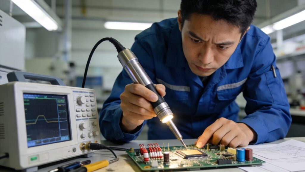
Step 5: Inspection & Testing
Comprehensive inspection ensures consistent quality.
AOI (Automated Optical Inspection)
Detects:
- Missing components
- Misalignment
- Solder bridges
- Polarity errors
X-ray Inspection for BGA
Used for hidden solder joints to detect:
- Voids
- Bridging
- Insufficient solder
ICT (In-Circuit Test)
Verifies:
- Resistance and capacitance
- Short circuits
- Open circuits
- Component performance
Functional Testing
Simulates real operating conditions to confirm:
- Electrical performance
- Firmware functionality
- Signal transmission
Testing significantly reduces field failure rates and warranty risks.
Step 6: Final Assembly & Packaging
After testing approval, products enter final integration.
Conformal Coating
Protects against:
- Moisture
- Dust
- Corrosion
- Chemical exposure
Ideal for automotive, medical, and industrial electronics.
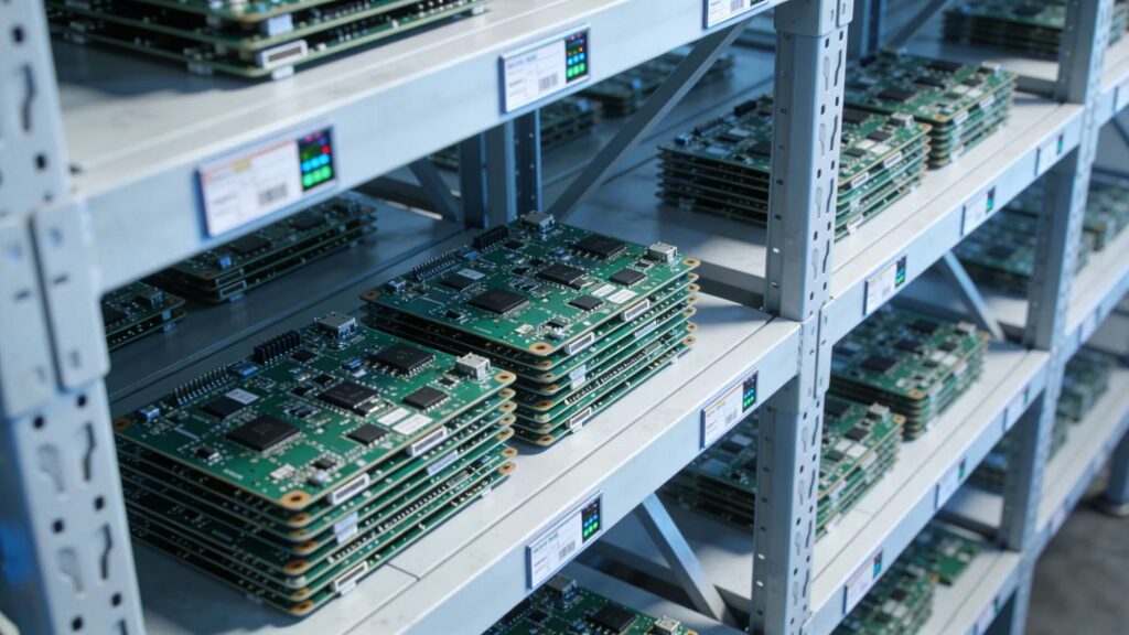
Box Build Assembly
Includes:
- Enclosure integration
- Cable harness installation
- Display module assembly
- Battery integration
Turnkey manufacturers provide full-system assembly services.
Custom Packaging
Professional packaging ensures:
- ESD protection
- Shock resistance
- Export compliance
This protects products during international shipping.
Quality Control Throughout the Process
Top-tier PCBA manufacturers implement multi-layer quality management systems.
Incoming Material Inspection (IQC)
- Component authenticity verification
- Random sampling
- Solderability testing
In-Process Quality Control (IPQC)
- Real-time production monitoring
- First article inspection
- Statistical process control
Final Quality Audit (FQA)
- Full appearance inspection
- Packaging verification
- Shipment approval
A structured QC system ensures consistent reliability across batches.
Why the PCBA Manufacturing Process Matters for Buyers
Understanding the complete workflow helps buyers:
- Evaluate supplier capability
- Compare technical strength
- Reduce defect risks
- Improve product launch success rate
- Ensure delivery stability
A transparent process is a key indicator of a professional and trustworthy PCBA partner.
Final Thoughts: Your Product Is Only as Strong as Your Manufacturing Partner
Behind every successful electronic product is a disciplined, standardized, and data-driven PCBA manufacturing process. From engineering review to final packaging, every step determines product reliability, brand reputation, and long-term profitability.
For OEM companies and global brands, choosing a manufacturer is not simply about price — it is about risk control, technical capability, quality assurance, and long-term cooperation potential.
A supplier with clear processes, advanced equipment, strong engineering support, and strict quality management can dramatically reduce project uncertainty and accelerate your time to market.
Why Yuxun Is a Reliable PCBA Partner
Yuxun integrates PCB assembly expertise with advanced intelligent manufacturing capabilities. With over 20 years of experience in electronic product development and manufacturing, the company provides:
- Professional DFM engineering support
- Advanced SMT production lines with high-precision placement
- Stable global component supply chain management
- Comprehensive AOI, X-ray, ICT, and functional testing systems
- One-stop turnkey PCBA and box build solutions
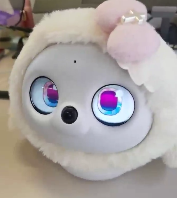
Yuxun specializes in high-end intelligent hardware and customized smart electronic products, helping global clients transform innovative ideas into stable, market-ready solutions.
If you are looking for a PCBA manufacturer that prioritizes quality, transparency, engineering strength, and long-term cooperation, partnering with an experienced company like Yuxun can give your project a decisive competitive advantage.
Your product deserves a manufacturing process you can trust.