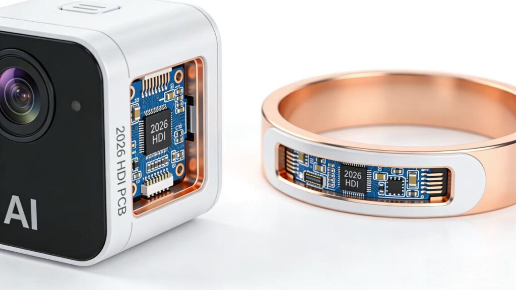
Electronic devices are becoming smaller, lighter, and more powerful every year. AI cameras now support ultra-high-resolution sensors. Smart speakers integrate multi-microphone arrays. Wearables such as smart rings pack sensors, batteries, and wireless modules into extremely limited space.
Traditional PCB designs often struggle to meet these requirements. Routing density becomes insufficient. Signal integrity may degrade. Power distribution can also become unstable.
This is where High Density Interconnect PCB (HDI PCB) technology becomes essential.
HDI boards allow electronic designers to place more components in smaller areas while maintaining signal quality and reliability. Advanced processes such as laser drilling microvias, sequential lamination, stacked microvias, and rigid-flex integration enable next-generation electronic products.
In this article, we will explore:
- What HDI PCB technology is and why it matters in 2026
- How microvia PCB and sequential lamination increase routing density
- Why HDI is critical for AI cameras, microphone arrays, and smart wearables
- The 2026 HDI market trends and manufacturing challenges
- How a professional HDI PCB board manufacturer like YUXUN supports advanced electronics development
For hardware engineers and product managers designing compact AI devices, understanding HDI technology is key to building competitive products.
What Is HDI PCB Technology?
HDI (High Density Interconnect) PCB refers to printed circuit boards that use advanced manufacturing technologies to achieve extremely dense wiring and compact layouts.
Compared with conventional PCBs, HDI boards feature:
- Microvia structures
- Higher layer counts
- Laser-drilled vias
- Sequential lamination
- Fine line and spacing
- Stacked or staggered vias
These technologies allow PCB designers to reduce board size while increasing performance.
Key Features of High Density Interconnect PCBs
A modern HDI PCB board manufacturer typically provides the following capabilities:
- Microvia diameter: 75–150 µm
- Trace/space: 50 µm or smaller
- Laser drilling for microvias
- Multi-layer sequential lamination
- Blind and buried vias
- Advanced impedance control
- High-speed signal integrity optimization
Because of these features, HDI boards are widely used in:
- AI cameras
- Smartphones
- wearable electronics
- smart rings
- AR/VR devices
- high-speed communication equipment
- medical electronics
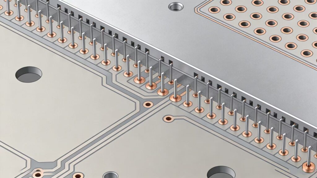
Core HDI Manufacturing Processes
To understand why HDI PCBs are powerful, we must examine their key manufacturing technologies.
Microvia PCB Technology: Laser-Drilled Connections
A microvia PCB uses very small vias to connect adjacent layers. Unlike traditional mechanical drilling, microvias are created using laser drilling technology.
Advantages of microvias include:
- Much smaller hole diameter
- Shorter electrical paths
- Reduced signal loss
- Higher routing density
- Improved reliability for high-speed circuits
Microvias typically connect only one or two layers, allowing designers to route signals more efficiently between dense components such as BGA packages.
For products like AI cameras or wireless modules, microvias significantly improve signal integrity.
Stacked and Staggered Microvia Structures
HDI PCBs support multiple microvia architectures.
Staggered Microvias
Vias are offset between layers.
Benefits:
- Lower manufacturing stress
- Higher reliability
- Lower cost
Stacked Microvias
Vias are stacked directly on top of each other.
Benefits:
- Extremely high density
- Shortest signal path
- Ideal for ultra-compact devices
Stacked microvias are common in advanced HDI PCB designs for wearables and mobile electronics.
Sequential Lamination: Enabling Ultra-High Density
Another essential HDI process is Sequential Lamination (SLP).
Instead of pressing all layers at once, HDI boards are laminated in multiple stages.
Common structures include:
- 1+N+1 HDI PCB
- 2+N+2 HDI PCB
- 3+N+3 HDI PCB
Example:
1+N+1 Structure
- One HDI layer on top
- Core multilayer board
- One HDI layer on bottom
This structure enables designers to integrate microvias and dense routing without increasing PCB size.
Sequential lamination allows high-performance routing for high-speed digital signals and complex component layouts.
Why HDI PCB Is Essential for Modern AI Devices
As electronic products evolve, HDI PCBs play a critical role in multiple industries.
Below are three representative application scenarios.
1.HDI for AI Cameras: Supporting High-Resolution Image Sensors

Modern AI cameras use large BGA image sensors with extremely high pin counts.
Challenges include:
- Dense signal routing
- High-speed data transmission
- Noise control
- limited PCB space
HDI technology solves these problems.
Advantages include:
- Direct routing under BGA packages
- shorter signal paths
- improved signal integrity
- better thermal management
With microvia PCB routing, high-resolution sensors can connect directly to image processors without long trace paths.
For applications such as:
- AI security cameras
- smart doorbells
- robotics vision systems
- industrial inspection cameras
HDI PCBs significantly improve performance and reliability.
2.HDI for AI Voice Products: Optimizing Microphone Arrays
Smart voice products rely heavily on microphone array PCBs.
Examples include:
- smart speakers
- voice assistants
- AI conference devices
- smart home controllers
These systems often use circular microphone array boards.
Key technical requirements:
- ultra-clean ground planes
- stable power distribution
- low noise
- high signal-to-noise ratio (SNR)
HDI PCBs allow engineers to design separate ground and power planes, improving electromagnetic performance.
Benefits include:
- reduced signal interference
- improved far-field voice pickup
- better voice recognition accuracy
For companies building next-generation AI smart speakers, HDI boards are now the preferred solution.
3.HDI Rigid-Flex PCB for Smart Rings and Wearables
Wearable electronics present one of the most challenging PCB design environments.
Devices such as smart rings must integrate:
- Bluetooth modules
- sensors
- batteries
- charging circuits
- microcontrollers
All within an extremely small curved structure.
The solution is Rigid-Flex HDI PCB technology.
Rigid-flex PCBs combine:
- rigid PCB sections
- flexible circuits
- HDI microvia routing
Advantages include:
- flexible form factor
- improved reliability
- reduced connector usage
- optimized space utilization
For smart rings, rigid-flex HDI boards can bend along the inner ring surface, maximizing internal space.
This design approach enables manufacturers to create ultra-compact wearable electronics.
2026 HDI PCB Market Trends
The demand for HDI technology continues to grow rapidly.
Key drivers include:
1. AI Hardware Expansion
AI devices require:
- high-speed signal routing
- dense chip integration
- compact design
HDI PCBs are essential for these requirements.
2. 5G and High-Speed Connectivity
5G and Wi-Fi 7 require PCBs with:
- controlled impedance
- low signal loss
- stable power distribution
HDI boards provide these capabilities.
3. Wearable Device Growth
Wearables such as:
- smart rings
- smart watches
- AR glasses
- medical monitoring devices
are pushing PCB miniaturization to new limits.
HDI and rigid-flex PCBs enable these innovations.
Challenges in HDI PCB Manufacturing
Despite its advantages, HDI production is technically demanding.
Key challenges include:
High-Precision Layer Alignment
Microvias must align perfectly between layers.
Any misalignment can cause electrical failure.
Yield Control
HDI boards involve:
- multiple lamination cycles
- laser drilling
- fine line etching
Manufacturing yield becomes a critical factor.
Advanced Equipment Requirements
HDI PCB production requires:
- laser drilling machines
- high-precision lamination systems
- advanced AOI inspection tools
Only experienced manufacturers can maintain consistent quality.
Why Choose YUXUN as Your HDI PCB Board Manufacturer
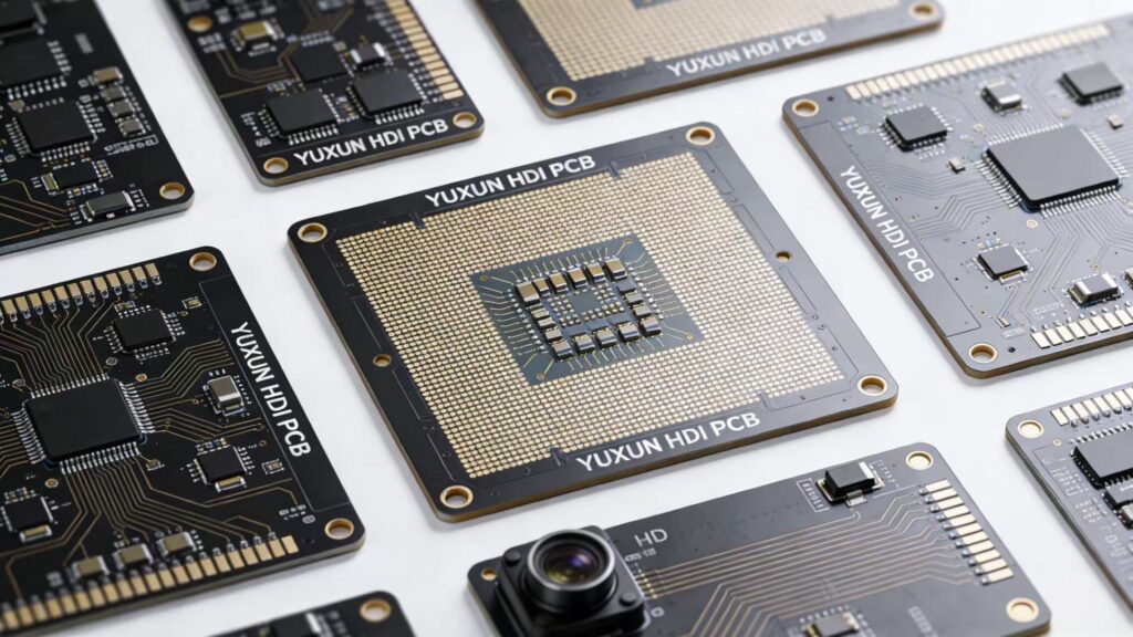
Choosing the right HDI PCB board manufacturer directly impacts product reliability and time-to-market.
YUXUN has built strong capabilities in advanced PCB manufacturing and customized electronics solutions.
Key advantages include:
Advanced HDI Manufacturing Capability
YUXUN supports:
- 1+N+1 / 2+N+2 HDI PCB structures
- laser-drilled microvia PCB
- stacked microvia technology
- high-speed signal routing
- impedance controlled multilayer PCBs
Strong Custom Design Support
The engineering team assists customers with:
- HDI layout optimization
- signal integrity design
- thermal management
- rigid-flex integration
This reduces design risks and accelerates product development.
One-Stop PCB and PCBA Service
YUXUN provides:
- PCB fabrication
- component sourcing
- SMT assembly
- functional testing
- mass production
This turnkey PCBA capability ensures consistent quality from prototype to large-scale production.
Experience in AI and Smart Device Applications
YUXUN has supported projects in:
- AI cameras
- voice recognition products
- wearable electronics
- IoT devices
This experience allows the team to deliver reliable HDI solutions for complex electronics.
Conclusion
As electronic products continue to shrink while adding more functionality, HDI PCB technology has become essential.
Technologies such as:
- microvia PCB
- stacked and staggered vias
- sequential lamination
- rigid-flex integration
enable engineers to design compact and powerful devices.
Applications like AI cameras, microphone arrays, and smart rings rely heavily on HDI boards to achieve high performance within limited space.
However, HDI manufacturing requires advanced equipment and deep engineering expertise.
Partnering with an experienced HDI PCB board manufacturer such as YUXUN ensures that complex designs can be produced with high reliability and consistent quality.
For companies developing the next generation of AI hardware and wearable devices, HDI technology will remain a key enabler of innovation.
FAQ: HDI PCB Technology
1. What is the difference between HDI PCB and standard PCB?
HDI PCBs use microvias, fine traces, and sequential lamination to achieve much higher circuit density. Standard PCBs rely on mechanically drilled vias and larger trace spacing.
2. What is a microvia PCB?
A microvia PCB uses laser-drilled vias with very small diameters. These vias connect adjacent layers and enable high-density routing in compact electronic devices.
3. Why are HDI PCBs used in AI cameras?
AI cameras use high-resolution image sensors and high-speed processors. HDI PCBs allow shorter signal paths, better signal integrity, and efficient routing under BGA packages.
4. What is a rigid-flex HDI PCB?
A rigid-flex HDI PCB combines rigid circuit boards with flexible circuits and high-density interconnect technology. It allows PCBs to bend while maintaining high wiring density.
5. How do I choose a reliable HDI PCB board manufacturer?
Look for manufacturers with:
- advanced HDI fabrication capability
- experience with microvia and stacked via structures
- strong engineering support
- strict quality control
- turnkey PCB assembly services
Manufacturers such as YUXUN specialize in customized HDI PCB solutions for advanced electronics.